Flip-Flops and Counters


Up until now, our digital circuits have been strictly combination -- they take inputs and react to them. While they are capable of complex calculations, they lack the ability to remember what they've done. This lack of memory severaly restricts the capabilities of the circuits we can design.
The flip-flop is the basic unit of digital memory. A flip-flop can remember one bit of data. Sets of flip-flops are called registers, and can hold bytes of data. Sets of registers are called memories, and can hold many thousands of bits, or more.
The basic flip-flop circuit is the classic set of cross-coupled NAND gates. Since nobody builds flip-flops from the gate level anymore, we'll skip past this level of analysis, and move straight into the chips we'll actually use. But if you're interested, The Art of Electronics devotes many pages to the inner workings of flip-flops, from the cross coupled NAND's on up.

  • D-flops

One of the most common kinds of flip-flops (or, just flops) is the D-type flop. Like all flops, it has the ability to remember one bit of digital information. What makes the D-flop special is that it is a clocked flip-flop. We'll spend some time looking at what that means.
First, let's go through the pins of a standard D-flop. The diagram above is for half of a 74HCT74 chip, which comes with two D-flops on one IC.
  • D is the Data Input pin. This is where the flop gets its information from.
  • Q is the Output pin. It shows what value the flop is currently remembering.
  • Q' is the Inverted Output pin. It shows the opposite of the value that the flop is remembering.
  • CLK is the clock pin. When a new clock pulse comes in, the flop checks the input pin D, and sets itself up to remember that input value. The D-flop is edge-triggere, which means that it responds to the rising edge of the clock pulse. This will be clearer when we look at a timing diagram, below.
  • R is an Active-LOW Reset pin. When the Reset pin gets a LOW signal, it resets the flop to remember a 0, or LOW value.
  • S (also called PRE on some diagrams) is an Active-Low Set pin. When it gets a LOW signal, it sets the flop to remember a 1, or HIGH value.
The flip-flop is the foundation of sequential logic. To understand how to use flops, we need to see how they function over time in response to different signals. We'll walk through a sequence, using a timing diagram to help show what's going on.
  • At the beginning of the diagram, the inputs to the D and CLK pins are LOW, and the Q output also happens to be LOW. At point A, the D input goes HIGH. However, since there is no clock pulse, the Q output does not change yet.
  • At point B, the CLK input sees a rising edge. That rising edge tells the flop to remember the D input.
  • A very short time passes from point B to point C, which is the time needed to actually make the flop remember the new value. Note that now the Q output is the same as the D input.
  • At point D, the D-input goes to LOW. However, the Q output does not change, because there is no clock pulse.
  • At point E, we have a falling edge on the CLK input. However, our flop only responds to rising edges, so the output Q still persists.
Note that the S and R pins will Set or Reset the flop regardless of the D input or clock pulses. These pins are often used to set the flop to an initial state before our logic circuits begin their work.
Here's the pin out of the 74HCT74N, a dual D-type flip-flop. Note that the 'dual' designation means that two flops come on one chip.


  • Switch Debounce

Having a component with memory can help us design circuits to solve a real variety of problems. To see how flexible flops are, we'll look at the problem of switch debounce.
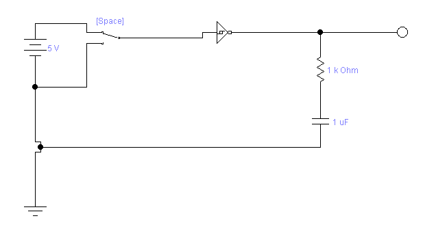
Consider this circuit, which is a fairly standard design for getting digital input from a push=button:
Now imagine what happens when we actually push button. We'd like the signal to have a sharp transition from LOW to HIGH, so it would look like this:
However, since the button is made of physical materials like metal, there will be some elastic vibrations, which result something like the following signal:

That switch bounce can wreak havoc on our edge triggered digital circuits, which can and will interpret each of the tiny peaks in the switch bounce as a new signal pulse.
We could get rid of the bounce by using a low-pass filter. However, this would slow down our response time, since we'd now have to allow for the RC curve.
Instead, we'll feed the output of our physical switch into a D-flop, and clock the flop with regular pulses from a 555 timer.
The timing diagram of the switch debouncer will look something like this:
The clock pulse should be fast enough to catch the shortest possible switch pressing, but slow enough not to be confused by the switch bounce, which typically lasts for about 1 ms. So, if we feed the flop with square waves that have a period of 1.5 ms, we'll satisfy both constraints.


  • Registers

One handy thing about flip-flops is that we can pack them onto chips pretty tightly. When we put 8 flops onto one chip, we have what's called a register. An 8-flop register can hold one byte of digital information.
Registers are very similar to normal D-flops, with a few differences. Here's a schematic diagram for a D-register:
Naturally, the D0 input feeds the Q0 output, and so on. You'll notice that all 8 of the D-flops are driven by a single clock input, marked with the triangle. They also share a single Reset pin. Registers make it handy to work with whole bytes at a time.
Often, we'll feed a register with inputs from a Data Bus. We'll talk more about the idea of the Data Bus later, but for now, we'll see that we don't have to draw 8 separate lines when we're feeding a byte into a register. Here's a convent schematic for an 8-bit bus:

The convention is that D0 will represent the lowest order (smallest) data bit, while D7 will represent the highest order (largest) bit.
Here's the pin out for an 74HCT273 register:


  • Flip-Flop Challenge

1. First, set up a push button switch to deliver a logic level input. View its output on a scope, and look at the switch bounce. Measure the duration of the switch bounce.
Then, set up a 555 timer that outputs a square wave with a period of 1.5 times the duration of the bounce for your switch. Finally, use that timer to drive a D-flop that debounces your switch. Use one of the flops on a 74HCT74N chip. View the debounced output on your scope next to the input. How much time delay is there between the input and output signals?
Make sure to tie S and R inputs HIGH (inactive).

Now, get a hold of a 74HCT273N D-register. Use the output of your debounced switch to clock the register. Attach 8 logic-level input switches to the D inputs of your register. Attach LED's, or a 7 segment LED to the Q outputs of your register. Remember to tie the R reset HIGH (inactive).
Experiment with your new circuit by pressing down different input buttons and then clocking your register with the debounced switch.
Then, add a logic level input switch to the R reset input. This input should be normally HIGH, but should output LOW when the switch is pressed. Experiment with this Reset button. Which takes priority for the chip, the clock pulse or the reset pulse?

  • Divide-by-2 Counter

Although it may seem obvious to say so, we can't count unless we have some kind of memory. The Divide-by-2 Counter is the first simple counter we can make, now that we have access to memory with flip-flops.
Here's the basic circuit:
Here, we're feeding the inverted output Q' into the D input. This means that every time we get a rising edge on the clock signal, our output will flip states.
So, clearly there's some division going on. But how do we interpret this as counting?
Let's look at what happens when we assign numbers to the voltage levels. 0 = LOW, 1 = HIGH.
Now, if we interpret the Clock levels as the 1's bit, and the Q out as the two's bit, we can see we've got a binary counter that counts from 0 to 3, and then resets.
So, our Divide-by-2 counter allows us to count clock pulses in a meaningful way. However, with one D-flop, we've got a severe limit on how high we can count. We need to find ways of counting past 4 if these circuits are going to be useful.


  • Ripple Counter

A good first thought for making counters that can count higher is to chain Divide-by-2 counters together. We can feed the Q out of one flop into the CLK of the next stage. The result looks something like this:
The ripple counter is easy to understand. Each stage acts as a Divide-by-2 counter on the previous stage's signal. The Q out of each stage acts as both an output bit, and as the clock signal for the next stage.
We can chain as many ripple counters together as we like. A three bit ripple counter will count 23=8 numbers, and an n-bit ripple counter will cound 2n numbers.
The problem with ripple counters is that each new stage put on the counter adds a delay. This propagation delay is seen when we look at a less idealized timing diagram:
Now we can see that the propagation delay does not only slow down the counter, but it actually introduces errors into the system. These errors increase as we add additional stages to the ripple counter.

  • Clocked Counters

To solve the problems of propagation delay introduced by the ripple counter, we'll use a synchronized counter. The synch'd counters are set up so that one clock pulse drives every stage. Since synch counters are readily available as cheap IC's, we'll move straight on to talk about how to use a counter chip.
A counter chip comes with a fair number of features on it. Here's the pinout for a 74HC193, which is a 4-bit binary up/down counter with load and clear.
Let's have a look at the different pins.
  • UP and DOWN. This counter chip has two clocks, UP and DOWN. When UP gets a rising edge clock pulse, it makes the internal flops count up by one number. When the DOWN pin gets a rising edge clock pulse, the flops count down by one number. If you're going to only use one clock pin, tie the other to ground.
  • Qa, Qb, Qcand Qd. These are the four output pins. Qa is the low order bit, Qd is the high order bit.
  • BO' and CO'. These pins stand for Borrow Out and Carry Out, respectively. They signal when the counter is about to reset. We can chain several of these counters together, by having the BO' pin drive the next counter's DOWN clock, and the CO' pin driving the next counter's UP clock.
  • CLR. This is a Clear pin, which will instantly reset all the outputs to LOW, or 0.
  • LOAD'. The LOAD' pin tells the chip to LOAD the data from pins A through D into outputs Qa to Qd on the next clock pulse. This allows us to start counting from a number other than zero.
  • ABCD. These four pins accept the input data, if we wish to set the counter to a certain number using the LOAD' pin.
  • As always, it's a good idea to tie any input pins we don't want to use to GND.
    As we mentioned, we can chain a series of counters together to form one big counter capable of handling as many digits as we like:
    Which of the Q's is the low order bit for the counter-system? Which of the Q's is the high order bit?

  • Counters Challenge
  • 1. Set up a Divide-by-2 counter using one D-flop from a 74HCT74N chip. Drive the counter with a square wave from a 555 Timer that you've set up to have a period of about half a second. Drive a red LED with the 555 Timer's square wave, and a green LED with the Q output from the D-flop.
    At what rate should the green LED blink? How can we interpret the green and red LED's as numbers?

    2. Add two more stages to the Divide-by-2 counter from above, making a 3-bit ripple counter. Drive an output LED with each Q outout, and watch it count happily.
    Now, use a scope to watch two of the Q outputs. Expand the time axis to see the propagation delay. How much delay is there per stage?

    3. Set up a synchronous counter using an SN74HC193N chip, or similar. Drive the UP and DOWN counters with straight (not-debounced) logic-level pushbutton inputs. Drive LED's from the Q-outputs.
    Click along with your pushbutton UP. What problems do you find using a not-debounced switch to clock the counter?

    4.Add a debouncer to the UP clock. Design and build a Divide-by-5 counter, using only the SN74HC193N, and the debounced UP input. The Divide-by-5 counter should light an LED every 5th time the user has pressed the UP pushbutton.

Comments

Popular posts from this blog

FREQUENCY DIVISION AND COUNTING

THE NOT SCHMITT TRIGGER (INVERTER)