Posts

Showing posts from 2014

THE NOT SCHMITT TRIGGER (INVERTER)

Image
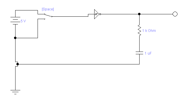
We can try and prove the function of The Not Schmitt Gate as Clock Generator with following this Circuit Diagram in ELECTRONIC WORK BENCH And these are several information about THE NOT SCHMITT TRIGGER Schmitt Trigger Characteristic :   The output is HIGH until the input rises to 66% of rail voltage. The output goes LOW when the input goes above 66%. The output remains HIGH until the input fall to 33%.  A Schmitt Trigger gate can be wired as an oscillator, delay, inverter (and other functions, depending on the surrounding components). Fig: 5 shows the Schmitt Trigger wired as an  oscillator ,  delay  and  inverter : Each of the 6 gates in the 74c14 can be used to create a separate "building block" and this gives the chip a wide range of capabilities.  Schmitt Inverter Waveform Generator This simple waveform generator circuit consists of a single TTL 74LS14 Schmitt inverter logic gate with a capacitor,  C  connected between its input terminal and

JOHNSON COUNTER

Image
A Johnson counter is a modified ring counter, where the inverted output from the last flip flop is connected to the input to the first. The register cycles through a sequence of bit-patterns. The MOD of the Johnson counter is 2n if n flip-flops are used. The main advantage of the Johnson counter counter is that it only needs half the number of flip-flops compared to the standard  ring counter  for the same MOD. The  switch-tail ring counter , also know as the  Johnson counter , overcomes some of the limitations of the ring counter. Like a ring counter a Johnson counter is a shift register fed back on its' self. It requires half the stages of a comparable ring counter for a given division ratio. If the complement output of a ring counter is fed back to the input instead of the true output, a Johnson counter results. The difference between a ring counter and a Johnson counter is which output of the last stage is fed back (Q or Q'). Carefully compare the feedback connection bel

RING COUNTER

Image
A ring counter is a Shift Register (a cascade connection of flip-flops) with the output of the last flip flop connected to the input of the first. It is initialized such that only one of the flip flop output is 1 while the remainder is 0. The 1 bit is circulated so the state repeats every n clock cycles if n flip-flops are used. The "MOD" or "MODULUS" of a counter is the number of unique states. The MOD of the n flip flop ring counter is n. It can be implemented using  D-type flip-flops  (or JK-type flip-flops). And this below, using the D Flip-flops    Enable the flips flops by clicking on the RESET (Green) switch. The RESET switch is a on/off switch (similar to a room light switch) Click on CLK (Purple) switch and observe the changes in the outputs of the flip flops. The CLK switch is a momentary switch (similar to a door bell switch - normally off). The D flip flop clock has a rising edge CLK input. For example Q 1  behaves as follows: The D input

Flip-Flops and Counters

Image
Up until now, our digital circuits have been strictly combination -- they take inputs and react to them. While they are capable of complex calculations, they lack the ability to remember what they've done. This lack of memory severaly restricts the capabilities of the circuits we can design. The flip-flop is the basic unit of digital memory. A flip-flop can remember one bit of data. Sets of flip-flops are called registers, and can hold bytes of data. Sets of registers are called memories, and can hold many thousands of bits, or more. The basic flip-flop circuit is the classic set of cross-coupled NAND gates. Since nobody builds flip-flops from the gate level anymore, we'll skip past this level of analysis, and move straight into the chips we'll actually use. But if you're interested,  The Art of Electronics  devotes many pages to the inner workings of flip-flops, from the cross coupled NAND's on up. D-flops One of the most common kinds of flip-flops (or,

FREQUENCY DIVISION AND COUNTING

Image
Each Flip Flop has its J and K inputs at the 1 level. so that It will change the states (toggle) whenever the signal on its CLK input goe from HIGH to LOW. The clock pulses are applied only to the CLK input of FF Qo. And the important things should be known and noted : FF Qo toggles on the negative-going transition of each input clock pulse FF Q1 toggles each time the Qo output goes from HIGH to LOW. FF Q2 toggles each time Q1 output goes from HIGH to LOW. Each FF output is a square wave (50 percent duty cycle)  Each FF divides the frequency of its inpt by 2. using the appropriate number of FFs, this circuit could divide a frequency power of 2. this application of flip-flops is referred to as frequency division. Counting Operation In addition to functioning as frequency divider, the circuit in figure 1 also operates as binary counter. State Transition Diagram Another way to show how the state of FFs change with each applied clock